(Hong Kong)

Product Summary
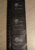
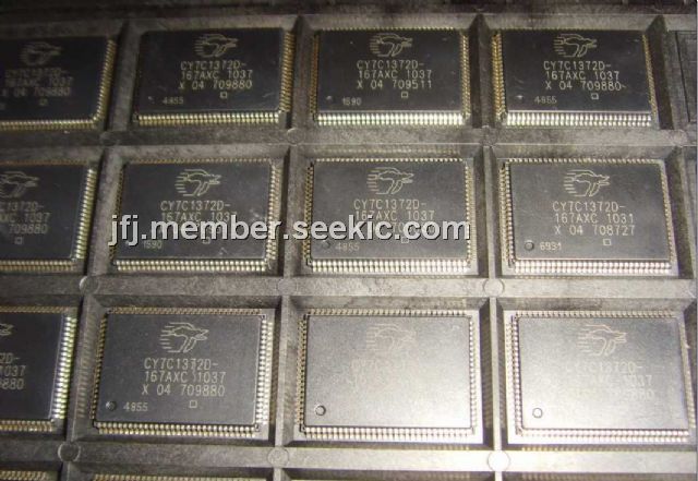
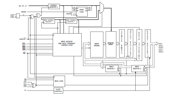
The CY7C1372D-167AXC is a 18 synchronous pipelined burst SRAM with No Bus Latency. It is designed to support unlimited true back-to-back read/write operations with no wait states. The CY7C1372D-167AXC is equipped with the advanced (NoBL) logic required to enable consecutive read/write operations with data being transferred on every clock cycle. This feature dramatically improves the throughput of data in systems that require frequent write/read transitions. The CY7C1372D-167AXC is pin compatible and functionally equivalent to ZBT devices.
Parametrics
CY7C1372D-167AXC absolute maximum ratings: (1)Storage Temperature: –65 ℃ to +150 ℃; (2)Ambient Temperature with Power Applied: –55 ℃ to +125 ℃; (3)Supply Voltage on VDD Relative to GND: –0.5 V to +4.6 V; (4)Supply Voltage on VDDQ Relative to GND: –0.5 V to +VDD; (5)DC to Outputs in Tristate: –0.5 V to VDDQ + 0.5 V; (6)DC Input Voltage: –0.5 V to VDD + 0.5 V; (7)Current into Outputs (LOW): 20 mA; (8)Static Discharge Voltage > 2001V; (9)Latch up Current > 200 mA.
Features
CY7C1372D-167AXC features: (1)Fully registered (inputs and outputs) for pipelined operation; (2)Byte write capability; (3)3.3 V core power supply (VDD); (4)3.3 V/2.5 V I/O power supply (VDDQ); (5)Fast clock-to-output times 2.6 ns (for 250 MHz device); (6)Clock enable (CEN) pin to suspend operation; (7)Synchronous self-timed writes; (8)Available in JEDEC-standard Pb-free 100-pin TQFP, Pb-free and non Pb-free 119-ball BGA and 165-ball FBGA package; (9)IEEE 1149.1 JTAG-compatible boundary scan; (10)Burst capability—linear or interleaved burst order.
Diagrams
| Image | Part No | Mfg | Description |  |
Pricing (USD) |
Quantity | ||||||||||||
|---|---|---|---|---|---|---|---|---|---|---|---|---|---|---|---|---|---|---|
 |
 CY7C1372D-167AXC |
Cypress Semiconductor |
SRAM 1Mx18 3.3V NoBL Sync PL SRAM COM |
Data Sheet |
|
|
||||||||||||
|
CY7C1372D-167AXCT |
Cypress Semiconductor |
SRAM 1Mx18 3.3V NoBL Sync PL SRAM COM |
Data Sheet |
|
|
||||||||||||