(Hong Kong)

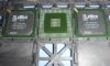
Product Summary
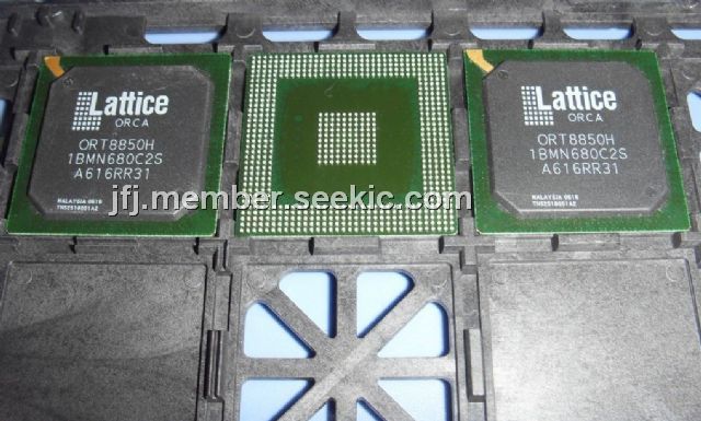
The ORT8850H-1BMN680C2S is a Field Programmable System-on-a-Chip (FPSC) brings a whole new dimension to programmable logic: Field Programmable Gate Array (FPGA) logic and an embedded system solution on a single device. Lattice has developed a solution for designers who need the many advantages of FPGA-based design implementation, coupled with high-speed serial backplane data transfer. Built on the Series 4 reconfigurable embedded System-on-a-Chip (SoC) architecture, the ORT8850H-1BMN680C2S is made up of backplane transceivers (SERDES) containing eight channels, each operating at up to 850 Mbits/s (6.8 Gbits/s when all eight channels are used). This is combined with a full-duplex synchronous interface, with built-in Clock and Data Recovery (CDR) in standard-cell logic, along with over 600K usable FPGA system gates.
Parametrics
ORT8850H-1BMN680C2S absolute maximum ratings: (1)Storage Temperature Tstg: -65 to 150 ℃; (2)VDD332: -0.3 to 4.2 V; (3)VDDIO: -0.3 to 4.2 V; (4)VDD15: -0.3 to 2.0 V; (5)VDDA_STM1: -0.3 to 2.0 V; (6)Input Signal with Respect to Ground: -0.3 VDDIO + 0.3 V; (7)Signal Applied to High-impedance Output: -0.3 VDDIO + 0.3 V; (8)Maximum Package Body (Soldering) Temperature: 220℃.
Features
ORT8850H-1BMN680C2S features: (1)Implemented in an ORCA Series 4 FPGA; (2)Allows a wide range of high-speed backplane applications, including SONET transport and termination; (3)No knowledge of SONET/SDH needed in generic applications. Simply supply data, 78 MHz—106 MHz clock, and a frame pulse; (4)High-Speed Interface (HSI) function for clock/data recovery serial backplane data transfer without external clocks; (5)Eight-channel HSI function provides 850 Mbits/s serial interface per channel for a total chip bandwidth of 6.8 Gbits/s (full duplex); (6)HSI function uses Lattice 850 Mbits/s serial interface core. Rates from 126 Mbits/s to 850 Mbits/s are supported ; (7)LVDS I/Os compliant with EIA?-644 support hot insertion. All embedded LVDS I/Os include both input and output on-board termination to allow long-haul driving of backplanes; (8)Low-power 1.5 V HSI core; (9)Low-power LVDS buffers; (10)Programmable STS-3, and STS-12 framing.
Diagrams
 |
 ORT82G5 |
Other |
|
Data Sheet |
Negotiable |
|
||||
|
ORT82G5-1BM680C |
Lattice |
Programmable Array Logic - Special 10368 LUT 372 I/O |
Data Sheet |
Negotiable |
|
||||
|
ORT82G5-1BM680I |
Lattice |
Programmable Array Logic - Special 10368 LUT 372 I/O |
Data Sheet |
Negotiable |
|
||||
|
ORT82G5-1F680C |
Lattice |
Programmable Array Logic - Special ORCA FPSC 3.7GBITS/s BP XCVR 643K |
Data Sheet |
Negotiable |
|
||||
|
ORT82G5-1F680I |
Lattice |
Programmable Array Logic - Special ORCA FPSC 2.7Gbits/s BP XCVR 643K |
Data Sheet |
Negotiable |
|
||||
|
ORT82G5-1FN680C |
Lattice |
Programmable Array Logic - Special ORCA FPSC 1.5V 3.7 G b Bpln Xcvr 643K Gt |
Data Sheet |
Negotiable |
|
||||